Week 8 · Communications · Lesson 16 of 24
DDS, LFSR and CRC on FPGAs: NCOs, PRBS and checksums
Build a DDS from a phase accumulator and sine table, a Galois LFSR with maximal-length taps and a byte-wide CRC-16 or CRC-32 in SystemVerilog, tested in Python.
What you will learn
- Calculate the tuning word, frequency resolution and phase truncation of a DDS
- Build a quarter-wave sine table and a pipelined NCO that matches a Python model bit for bit
- Write a Galois LFSR, choose maximal-length taps and check the period in simulation
- Compute a CRC by polynomial division and describe a CRC by its width, poly, init, refin, refout and xorout
- Implement a byte-wide parallel CRC and verify it with the standard check value
Before you start
- Memory and DSP (lesson 14)
- Self-checking testbenches (lesson 9)
- Python verification with cocotb (lesson 10)
After this lesson you can generate a sine wave of any frequency from a fixed clock, produce long pseudo-random bit sequences from a few flip-flops, and add an error check to a data link. Each design is checked bit for bit against a Python model.
Where these blocks are used
The Week 8 lab of this course adds a CRC to the UART link, so a receiver can reject corrupted frames. The NCO from this lesson can generate the carrier for the modulators in digital modulation, and an LFSR can supply test data for either link. None of the three needs a DSP slice.
Direct digital synthesis
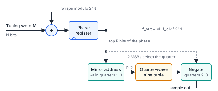
A direct digital synthesiser (DDS) makes a sine wave from a fixed clock. The digital part, without the DAC, is called a numerically controlled oscillator (NCO). It has two stages: a phase accumulator, and a phase-to-amplitude converter, usually a sine lookup table.
Phase accumulator and the tuning equation
The phase accumulator is an N-bit register that adds the tuning word M on every clock. Its value is the phase of the output, where the full range stands for one cycle, 360 degrees. The register wraps modulo , so it completes one cycle every clocks, so the output frequency is
This is the DDS tuning equation as given in the Analog Devices tutorial MT-085. The smallest step, with M = 1, is the frequency resolution .
The Nyquist limit applies: must stay below . MT-085 puts the practical limit at about a third of the clock. The filter after the DAC must pass and remove the image at , and the two move closer together as rises. Harmonics of the output also fold back into the band below , where no filter can remove them.
Worked example: frequency resolution
Take a 100 MHz clock and a 32-bit accumulator.
- Resolution: Hz.
- Tuning word for 1 kHz: , which is
32'h0000A7C6. - Actual output: Hz, an error of 7.6 mHz.
- Tuning word for 1 MHz: , giving Hz.
A wider accumulator costs only adder bits, which use the carry chain. That is why wide accumulators are common: the DDS block diagram in MT-085 shows 24 to 48 bits. Changing M changes the frequency on the next clock without a phase jump, because the accumulator keeps its value.
From phase to amplitude
Only the top P bits of the phase address the sine table. Dropping the lower bits is called phase truncation. It keeps the table small and does not change the frequency resolution, which depends only on N.
A full table with P = 10 holds 1024 words. A sine wave has quarter-wave symmetry, so a table of the first quarter is enough, as MT-085 also notes:
| Phase quarter (top 2 bits) | Table address | Sign |
|---|---|---|
| 00: 0 to 90 degrees | a | + |
| 01: 90 to 180 degrees | mirrored, ~a | + |
| 10: 180 to 270 degrees | a | - |
| 11: 270 to 360 degrees | mirrored, ~a | - |
The design samples the sine half a step off zero: entry k holds . With that offset the quarter is exactly symmetric, so the mirrored address is a bitwise NOT, with no subtraction. The table shrinks from 1024 to 256 words of 16 bits, which fits a single block RAM or a small LUT ROM. The table file is generated by dds_model.py, the same model the tests use. The ROM coding pattern is the one from memory and DSP: an array, $readmemh in an initial block and a synchronous read.
Phase truncation and spurs
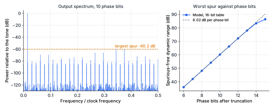
Truncation adds a phase error that repeats with a pattern set by the dropped bits. A repeating error is not noise: it shows up as discrete spurious tones, spurs. The spurious-free dynamic range (SFDR) is the distance from the carrier to the largest spur.
The figure was computed from the Python model of this lesson’s design. The tuning word, , makes the dropped bits cycle through 64 values. The SFDR rises by about 6 dB per extra phase bit, from 36.0 dB at 6 bits to 78.0 dB at 13 bits. Above that, the 16-bit amplitude rounding of the table limits the result. The 10-bit design here has an SFDR of 60.2 dB with this tuning word. It is not the worst case: when the dropped bits of the tuning word are exactly half a table step, the truncation error alternates between zero and its largest value, and the model’s SFDR at 10 bits falls to 56.3 dB. If the phase starts at zero and the tuning word is a multiple of (with N = 32 and P = 10), the dropped bits stay zero and there is no truncation error at all.
For the amplitude quantisation error, MT-085 describes two further measures: choose a ratio of clock to output frequency that spreads the error, or add a small pseudo-random dither before the DAC. An LFSR, the next topic, is a cheap source for that pseudo-random sequence.
The DDS in SystemVerilog
dds.sv registers the phase, then the mirrored table address, then the table output, then the signed sample. Each stage is a single register, so the table read is synchronous and the negation sits in its own cycle:
assign ph_t = phase[ACC_W-1 -: PH_W];   // top PH_W bits of the phase

always_ff @(posedge clk) begin
    if (rst)     phase <= '0;
    else if (en) phase <= phase + tuning_word;
end

always_ff @(posedge clk) begin
    addr1  <= ph_t[AW] ? ~ph_t[AW-1:0] : ph_t[AW-1:0];  // mirror in quarters 1 and 3
    neg1   <= ph_t[PH_W-1];                             // quarters 2 and 3 are negative
    mag2   <= lut[addr1];                               // synchronous table read
    neg2   <= neg1;
    sample <= neg2 ? -$signed(mag2) : $signed(mag2);
end
The latency from the phase register to sample is three clocks, and sample_valid follows the data. The cocotb test cocotb_dds.py checks two things. First, a steady 1 MHz tone must match dds_model.dds_samples() sample for sample. Second, with random tuning words and random gaps in en, every phase step must equal the tuning word, and every sample must equal the model’s value for the phase three cycles earlier.
dds.sv
Download dds_sine_quarter.hex
Download dds_model.py
Download cocotb_dds.py
Download test_cocotb_dds.py
Linear feedback shift registers
A linear feedback shift register (LFSR) is a shift register whose input is an XOR of some of its own bits. With the right feedback taps, a W-bit LFSR steps through all non-zero states before it repeats. The state sequence looks random but is fully determined by the taps and the starting value, the seed.
Fibonacci and Galois forms
There are two ways to wire the same feedback polynomial.
- Fibonacci (external XOR): the tapped bits are XORed together and the result enters the first cell. With four taps, the feedback is a four-input XOR in front of one flip-flop.
- Galois (internal XOR): the bit leaving the register is XORed into each tapped position as the bits shift past. Each cell has at most one two-input XOR in front of it, whatever the number of taps.
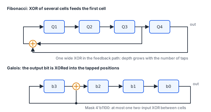
For the same taps both forms have the same period, but the order of the states differs. On an FPGA a four-input XOR fits in one LUT, so the difference is small for few taps. The Galois form keeps one gate of depth as taps are added and is easy to parameterise with a mask.
XAPP052 builds its counters with XNOR feedback. With XNOR the state that never changes, the lock-up state, is all ones; with XOR it is all zeros. This lesson uses XOR, so the seed must not be zero.
Maximal-length taps
A tap set gives the full period only when its feedback polynomial is primitive. Copy taps from a table and check them. The rows below come from Table 3 of XAPP052, which lists taps for 3 to 168 bits with the bits numbered 1 to n. The Galois mask has bit t-1 set for every tap t.
| Width | XAPP052 taps | Galois mask | Period |
|---|---|---|---|
| 4 | 4, 3 | 4'hC | 15 |
| 7 | 7, 6 | 7'h60 | 127 |
| 8 | 8, 6, 5, 4 | 8'hB8 | 255 |
| 10 | 10, 7 | 10'h240 | 1 023 |
| 16 | 16, 15, 13, 4 | 16'hD008 | 65 535 |
| 24 | 24, 23, 22, 17 | 24'hE10000 | 16 777 215 |
| 32 | 32, 22, 2, 1 | 32'h80200003 | 4 294 967 295 |
test_lfsr_model.py checks every row twice: by counting the period for widths up to 16, and by a primitivity test of the polynomial that works for 32 bits. The 24-bit and 32-bit rows were also counted once by brute force. The testbench tb_lfsr.sv builds one LFSR for every width from 3 to 16 and checks that each returns to its seed after exactly clocks without reaching zero.
The lfsr module
module lfsr #(
    parameter int           W    = 16,
    parameter logic [W-1:0] MASK = 16'hD008,
    parameter logic [W-1:0] SEED = 1
) (
    input  logic         clk,
    input  logic         rst,     // synchronous, active high: load SEED
    input  logic         en,
    output logic [W-1:0] state,
    output logic         bit_out
);
    always_ff @(posedge clk) begin
        if (rst)     state <= SEED;
        else if (en) state <= state[0] ? ((state >> 1) ^ MASK) : (state >> 1);
    end
    assign bit_out = state[0];
endmodule
cocotb_lfsr.py builds the module as a 32-bit LFSR and compares 5000 states, with random gaps in en, against lfsr_model.galois_step().
What LFSRs are used for
- Test patterns. A pseudo-random bit sequence (PRBS) exercises a serial link with every non-zero W-bit pattern. The receiver runs an identical LFSR and counts mismatches. XAPP052 presents its long generators for testing.
- Dither. MT-085 adds about half an LSB of pseudo-random dither to a DDS output to break up the spur pattern.
- Counters. When only the terminal count matters, an LFSR replaces a binary counter. XAPP052 uses LFSR counters to address its RAM-based shift registers.
An LFSR is not a secure random number generator. Its next state is a linear function of the current one, and the W cells of a Fibonacci LFSR hold W consecutive output bits. Anyone who knows the taps and sees W consecutive bits can predict the rest. The hardware security lesson covers true random number generators.
Cyclic redundancy checks
A CRC is a short check value computed from a message. The sender appends it and the receiver recomputes it; if the values differ, the frame is corrupted. The hardware is the same shift register and XOR gates as an LFSR.
Polynomial division
Treat the message bits as the coefficients of a polynomial over GF(2), where addition and subtraction are both XOR and there are no carries. For a W-bit CRC with generator polynomial G(x) of degree W:
- Append W zero bits to the message, which multiplies it by .
- Divide by G(x) using XOR instead of subtraction.
- The W-bit remainder is the CRC. Sending the message followed by the remainder gives a codeword that G(x) divides exactly.
A small example with (binary 1011) and the message 1101:
1101000     message with 3 zeros appended
1011        XOR where the leading bit is 1
0110000
 1011
0011100
  1011
0001010
   1011
0000001     remainder = 001
The CRC is 001 and the codeword is 1101001. Dividing the codeword by 1011 leaves zero.
What a CRC detects
The receiver sees the codeword plus an error pattern E(x). The error goes undetected only if G(x) divides E(x). Two results follow from that directly:
- A single-bit error is . Any G(x) with two or more terms cannot divide it, so every single-bit error is detected.
- A burst error of length W or less is with B(x) of degree below W and a constant term. If G(x) has a term, it shares no factor with and cannot divide B(x), which has lower degree. So every burst up to W bits long is detected.
Other properties depend on the polynomial. If is a factor of G(x), every error with an odd number of flipped bits is detected: such an E(x) equals 1 at x = 1, while G(1) = 0. The CRC-16 polynomial has an even number of terms, so G(1) = 0 and it has this property. Use a polynomial from a standard rather than inventing one.
Parameters and check values
The CRC used in a protocol is not fixed by the polynomial alone. The RevEng CRC catalogue describes each algorithm with six parameters:
- width and poly: register size and generator, written without the top term (
0x1021for ). - init: the register value before the first bit.
- refin: whether each byte is read LSB first (true) or MSB first (false).
- refout: whether the register is bit-reversed before output.
- xorout: a value XORed into the result at the end.
Every catalogue entry also gives check, the CRC of the nine ASCII bytes "123456789". If your implementation reproduces the check value, the parameters are almost certainly right.
| Name in the catalogue | Width | poly | init | refin/refout | xorout | check |
|---|---|---|---|---|---|---|
| CRC-8/SMBUS | 8 | 0x07 | 0x00 | false | 0x00 | 0xF4 |
| CRC-16/IBM-3740 (alias CRC-16/CCITT-FALSE) | 16 | 0x1021 | 0xFFFF | false | 0x0000 | 0x29B1 |
| CRC-16/XMODEM | 16 | 0x1021 | 0x0000 | false | 0x0000 | 0x31C3 |
| CRC-16/KERMIT | 16 | 0x1021 | 0x0000 | true | 0x0000 | 0x2189 |
| CRC-32/ISO-HDLC (alias CRC-32) | 32 | 0x04C11DB7 | 0xFFFFFFFF | true | 0xFFFFFFFF | 0xCBF43926 |
The three 16-bit rows share one polynomial and still give three different results. The catalogue notes that CRC-16/IBM-3740 is often misidentified as “CRC-CCITT”. When a data sheet says only “CRC-CCITT”, ask for a test vector.
Reflected CRCs read each byte LSB first. That matches links that send the LSB first, such as the UART in lesson 17.
Serial and byte-wide hardware
The serial form shifts one message bit per clock. The bit entering is XORed with the bit leaving the top of the register, and if the result is 1 the polynomial is XORed in. This is the long division above, done one step per clock:
assign fb = crc_out[W-1] ^ bit_in;

always_ff @(posedge clk) begin
    if (rst || start)   crc_out <= INIT;
    else if (bit_valid) crc_out <= fb ? ((crc_out << 1) ^ POLY) : (crc_out << 1);
end
A UART delivers a whole byte at once, and a wider data path may deliver several bytes per clock. A byte-wide CRC runs eight serial steps in one clock. Writing those steps as a loop in a function lets the synthesis tool unroll them into an XOR network: each new register bit becomes the XOR of a fixed set of old register bits and data bits. No table and no DSP slice is needed.
function automatic logic [W-1:0] crc_byte(input logic [W-1:0] c, input logic [7:0] d);
    logic [W-1:0] r;
    logic         fb;
    r = c;
    for (int i = 7; i >= 0; i--) begin
        fb = r[W-1] ^ d[i];
        r  = r << 1;
        if (fb) r = r ^ POLY;
    end
    return r;
endfunction

assign din     = REFIN ? rev8(data) : data;
assign crc_out = (REFOUT ? revw(reg_q) : reg_q) ^ XOROUT;
crc.sv takes the six catalogue parameters as module parameters. Its defaults give CRC-16/IBM-3740. A start input loads init and can coincide with the first byte, so messages can follow back to back. The register stays in unreflected form; reflection is only rewiring and costs no logic.
For wider data paths the same function loops over more bits. The XOR trees grow and may need pipelining at high clock rates. The serial and parallel forms must give the same result, which makes the serial form a reference for testing.
Testing the CRC
Three tests cover the CRC block:
tb_crc.svsends"123456789"twice throughcrc.svconfigured as CRC-8/SMBUS, CRC-16/IBM-3740 and CRC-32/ISO-HDLC, and once bit by bit throughcrc_serial.sv. It checks all four against the catalogue check values.crc_model.pyis checked against the catalogue values and against the CRC routines in Python’s standard library:zlib.crc32computes CRC-32/ISO-HDLC, andbinascii.crc_hqxwith an initial value of 0 or 0xFFFF computes CRC-16/XMODEM or CRC-16/IBM-3740.cocotb_crc.pybuildscrc.svin all three configurations and compares 100 random messages per build (one of them empty, with random idle cycles between bytes) against the model.
iverilog -g2012 -o sim tb_crc.sv crc.sv crc_serial.sv && vvp sim
# CRC-16/IBM-3740 = 000029b1
# CRC-32/ISO-HDLC = cbf43926
# CRC-8/SMBUS = 000000f4
# ...
# PASS
python -m pytest -q # models, cocotb DDS, LFSR and CRC testslfsr.sv
Download tb_lfsr.sv
Download lfsr_model.py
Download crc.sv
Download crc_serial.sv
Download tb_crc.sv
Download crc_model.py
Download cocotb_crc.py
Download test_cocotb_crc.py
Download cocotb_lfsr.py
Download test_cocotb_lfsr.py
Tune a DDS for an audio tone
A DDS runs from a 50 MHz clock with a 28-bit phase accumulator and a 10-bit truncated phase, as in dds.sv with ACC_W = 28.
- What is the frequency resolution?
- Which tuning word gives the closest frequency to 440 Hz, and what frequency does it produce?
- Does reducing
PH_Wfrom 10 to 8 change your answers? What does it change?
Show solution
- Hz.
- . The output is Hz, 0.043 Hz low.
- No. Resolution and frequency depend only on the accumulator width and the clock. Two fewer phase bits shrink the quarter table from 256 to 64 words and raise the worst truncation spur by about 12 dB, from about -60 dBc to about -48 dBc in the model. You can check the last numbers with
dds_model.dds_samples(..., phase_bits=8)and an FFT.
A CRC by hand and in hardware
- Compute the 3-bit CRC of the message
10110011with by long division. - Which parameters of
crc.svgive CRC-16/KERMIT, and which check value should your testbench expect?
Show solution
- Append three zeros,
10110011000, and divide by1011. The remainder is101, so the codeword is10110011101. You can confirm it in Python: the remainder of0b10110011000divided by0b1011over GF(2) is0b101. W = 16,POLY = 16'h1021,INIT = 16'h0000,REFIN = 1'b1,REFOUT = 1'b1,XOROUT = 16'h0000. The catalogue check value is0x2189, andcrc_model.pyreproduces it.
Summary
- A DDS adds a tuning word M to an N-bit phase accumulator every clock. The output frequency is and the resolution is .
- Only the top P phase bits address the sine table. A quarter-wave table with a mirrored address and a sign stage needs a quarter of the memory. Each phase bit dropped raises the worst truncation spur by about 6 dB.
- A Galois LFSR shifts right and XORs a tap mask into the state when the bit leaving is 1. With taps from a verified table it visits all non-zero states; all zeros is the XOR lock-up state.
- A CRC is the remainder of polynomial division over GF(2). Specify it by width, poly, init, refin, refout and xorout, and test it with the catalogue check value for
"123456789". - A byte-wide CRC is the serial CRC loop unrolled eight times in a function. Synthesis turns it into one XOR network per register bit.
Check your understanding
Pick an answer for each question, then check. Answers stay hidden until you submit.
Further reading
- Documentation
- Documentation
- Documentation
- Paper
Found a mistake or something unclear?Report a correction.
Follow this course
Get an email when new lessons and projects are added to this course.