Weeks 1–2 · Introduction and architecture · Lesson 1 of 24
What is an FPGA? Programmable hardware explained
What an FPGA is, how it differs from a microcontroller, an ASIC and a GPU, where FPGAs are used, the main vendors, and how the configuration is stored.
What you will learn
- Explain what a field-programmable gate array is and how it differs from a processor running software
- Compare FPGAs with microcontrollers, ASICs and GPUs for a given application
- Name the main FPGA vendors and the kind of devices each one sells
- Describe the difference between SRAM, flash and antifuse configuration
Before you start
- Basic digital logic: gates, flip-flops, binary numbers
By the end of this lesson you will be able to say what an FPGA is, decide when one is a better choice than a microcontroller, an ASIC or a GPU, and recognise the main vendors and configuration technologies you will meet in datasheets and job adverts.
Hardware you can rewrite
FPGA stands for field-programmable gate array. It is a chip with a large grid of identical logic blocks, programmable wires between them, and input/output (I/O) blocks around the edge. None of these parts has a fixed function when the chip leaves the factory. You decide what they do, and you can change it later “in the field”, after the board has been built.
Each logic block contains look-up tables (LUTs), which can implement any Boolean function of a few inputs, and flip-flops, which store one bit each. The routing network connects the output of any block to the inputs of other blocks through programmable switches. Most modern FPGAs also include columns of dedicated blocks that would be wasteful to build from LUTs: block RAM for memory and DSP blocks for multiplication.
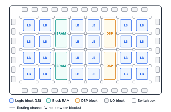
The setting of every LUT and routing switch is held in configuration memory, which is filled from a file called a bitstream. Load a different bitstream and the same chip becomes a different circuit. Lesson 2 covers each block in detail.
Programmable hardware versus a processor
A microcontroller is also “programmable”, but in a different sense. Its hardware is fixed: a processor core fetches instructions from memory and executes them one after another on a fixed datapath. Your program changes the sequence of instructions, not the circuit.
On an FPGA you do not write instructions. You describe a circuit in a hardware description language (HDL) such as Verilog, SystemVerilog or VHDL, and the tools turn that description into a configuration for the fabric. Every part of the circuit runs at the same time, because it is separate hardware.
Worked example: counting bits
Counting the number of 1 bits in a byte (a “population count”) shows the difference. In software you would loop over the bits:
count = 0;
for (i = 0; i < 8; i++)
    count += (data >> i) & 1;
The processor executes this loop step by step, so the time it takes grows with the number of bits. On an FPGA you build an adder tree instead. Four small adders sum pairs of bits, two adders sum those results, and one final adder produces the count. All seven adders exist as hardware and work in parallel.
module popcount8 (
  input  logic [7:0] data,
  output logic [3:0] count
);
  logic [1:0] s0, s1, s2, s3;   // pair sums, 0..2
  logic [2:0] t0, t1;           // sums of pairs, 0..4

  assign s0 = {1'b0, data[0]} + {1'b0, data[1]};
  assign s1 = {1'b0, data[2]} + {1'b0, data[3]};
  assign s2 = {1'b0, data[4]} + {1'b0, data[5]};
  assign s3 = {1'b0, data[6]} + {1'b0, data[7]};

  assign t0 = {1'b0, s0} + {1'b0, s1};
  assign t1 = {1'b0, s2} + {1'b0, s3};

  assign count = {1'b0, t0} + {1'b0, t1};  // 0..8
endmodule
The result is ready a few gate delays after data changes, so a new byte can be processed every clock cycle. Sixteen counters are sixteen copies running at once, where a processor would share one datapath between them. The testbench checks all 256 input values against a software-style reference model. Lesson 4 teaches the language; for now, notice that the code describes structure, not a sequence of steps.
popcount8.sv
Download tb_popcount8.sv
FPGA, microcontroller, ASIC or GPU
Four kinds of chip compete for most digital processing jobs. The table compares them in general terms. Exact figures depend heavily on the specific device and process node, so the table gives directions rather than numbers.
| Microcontroller | FPGA | ASIC | GPU | |
|---|---|---|---|---|
| What you change | Software instructions | The circuit (configuration bits) | Nothing after fabrication | Software kernels |
| Parallelism | One or a few cores | As much as fits in the fabric | Designed in, fixed | Thousands of identical threads |
| Timing | Depends on code paths and interrupts | Cycle-exact and deterministic | Cycle-exact and deterministic | Throughput-oriented; latency varies |
| I/O | Fixed peripherals | Almost any pin can be any interface | Designed in | Through a host bus |
| Up-front cost | Very low | Low (tools often free) | Very high (masks, verification) | Low |
| Cost per unit | Lowest | Moderate to high | Lowest at high volume | High |
| Performance per watt on a custom task | Low | Medium | Highest | High for data-parallel work |
| Typical use | Control, user interfaces, sensors | Custom datapaths, low latency, unusual I/O | Mass-market products | Large data-parallel maths, graphics, neural networks |
FPGA versus ASIC. An application-specific integrated circuit (ASIC) is a chip fabricated for one design. It contains only the gates it needs, with fixed wires between them, so it runs faster and uses less area and power than the same design on an FPGA. The price is a large one-time cost for masks and verification, months of fabrication, and a new mask set for any bug found afterwards. FPGAs win at low to moderate volume, when the design must change after shipping, or when time to market matters. Kuon and Rose measured this gap for a set of benchmark circuits, comparing a 90 nm FPGA with 90 nm standard-cell ASICs. For circuits built only from LUTs and flip-flops, the FPGA needed on average 35 times the silicon area, its critical path was 3.4 times slower, and it used 14 times the dynamic power. Hard memory and multiplier blocks reduced the area gap to as little as 18 times. Their paper is listed under further reading.
FPGA versus microcontroller. If a task fits comfortably in software on a microcontroller, use the microcontroller: it is cheaper and easier to debug. Choose an FPGA when many operations must happen in the same clock cycle, timing must be exact to the nanosecond, or no microcontroller peripheral provides the I/O you need. Some FPGAs include hard processor cores on the same die (AMD Zynq, Altera SoC FPGAs, Microchip PolarFire SoC).
FPGA versus GPU. A GPU runs the same instruction on many data elements at once, which suits large floating-point workloads such as training neural networks. It works on batches in memory behind a host bus, so latency for one small input is high and varies. An FPGA processes a stream sample by sample as it arrives on its pins, with fixed latency and custom number formats.
Where FPGAs are used
FPGAs appear wherever volume is low to medium, hardware must be updated after shipping, I/O bandwidth is very high, or latency must be low and fixed.
- Communications. Base stations, network switches and optical transport equipment process packets and signals at line rate. Standards change often, and reprogrammable hardware can follow them.
- Test and measurement. Oscilloscopes and protocol analysers must process every sample from fast converters in real time.
- ASIC prototyping. A large chip’s RTL is mapped onto one or more FPGAs so firmware teams can run real software before silicon exists.
- Video and imaging. Broadcast equipment, machine vision cameras and medical imaging systems run pixel pipelines with many parallel streams.
- Data centre acceleration. Cloud providers offer servers with FPGA accelerator cards, and FPGAs offload packet processing in network interface cards.
- Aerospace and defence. Satellites, radar and avionics have low volumes and long lifetimes. Radiation-tolerant FPGA families exist for space.
Industrial motor control, automotive driver assistance and scientific instruments use them too.
Vendors and device families
A handful of companies make almost all FPGAs. Each sells several families aimed at different points on the cost and performance scale. Product lines change often, so check the vendor website for current parts.
| Vendor | Example families | Positioning |
|---|---|---|
| AMD (formerly Xilinx) | Spartan, Artix, Kintex, Virtex, Zynq, Versal | Full range, from low-cost devices to the largest FPGAs and adaptive SoCs with Arm cores |
| Altera | MAX 10, Cyclone, Arria, Stratix, Agilex | Full range; owned by Intel for several years and now operating as a separate company again |
| Lattice Semiconductor | iCE40, MachXO, ECP5, CrossLink-NX, Certus-NX | Small, low-power and low-cost devices; strong open-source toolchain support for iCE40 and ECP5 |
| Microchip (Microsemi, formerly Actel) | PolarFire, PolarFire SoC, IGLOO 2, SmartFusion 2, RTG4 | Non-volatile, low-power devices and radiation-tolerant families for space |
| Efinix | Trion, Titanium | Low- to mid-range devices built on its own fabric architecture |
| Gowin Semiconductor | LittleBee, Arora | Low-cost devices; open-source support through Project Apicula |
AMD and Altera dominate the high end. Lattice, Microchip, Efinix and Gowin focus on lower cost, lower power or specific markets. The concepts in this course apply to all of them. Where a step depends on the tool, lessons show AMD Vivado and Altera Quartus Prime, and the open-source Yosys and nextpnr flow where it applies.
How the configuration is stored
The configuration memory can be built from three kinds of cell. The choice affects power-up behaviour, security, radiation tolerance and whether you can reprogram the part.
SRAM-based
Most FPGAs, including the large AMD and Altera families, Lattice iCE40 and ECP5, and Efinix devices, store their configuration in SRAM cells. SRAM uses the same manufacturing process as the logic, so these devices get the newest process nodes first. SRAM is volatile, so at every power-up the FPGA loads its bitstream from an external flash chip or a host processor before the design starts. A charged particle can occasionally flip a configuration bit and change the circuit (a single-event upset). Designs for harsh environments detect this and periodically rewrite the configuration (“scrubbing”).
Flash-based
Microchip’s PolarFire and IGLOO families build their configuration switches from non-volatile flash cells. The device is live as soon as power is stable, needs no external configuration memory, and its configuration cells are far less susceptible to radiation-induced upsets than SRAM. Flash cells can be reprogrammed only a limited number of times, and flash processes tend to lag behind the newest process nodes used for SRAM-based parts.
Some devices take a middle path. Altera MAX 10 and Lattice MachXO2 and MachXO3LF devices keep SRAM configuration cells but add on-chip flash that loads them at power-up. Several Gowin LittleBee devices also include on-chip configuration flash. From the board designer’s point of view these are single-chip, non-volatile parts.
Antifuse
An antifuse starts as an open circuit, and programming forms a permanent conductive link. Antifuse FPGAs are one-time programmable, very resistant to radiation, and live at power-up. These properties suit space and defence systems, where antifuse parts from Microchip (originally Actel) have been used. Elsewhere, one-time programming makes development slow and costly.
| SRAM | Flash | Antifuse | |
|---|---|---|---|
| Reprogrammable | Yes, unlimited | Yes, limited write cycles | No, once only |
| Keeps configuration without power | No | Yes | Yes |
| Needs external configuration memory | Usually | No | No |
| Live at power-up | After loading | Yes | Yes |
| Configuration upsets from radiation | Possible | Rare | Very rare |
What this course covers
The course follows the path a design takes from idea to working hardware.
- Foundations. How the fabric is built (FPGA architecture) and the steps from source code to programmed chip (the design flow).
- HDL for synthesis. Verilog and SystemVerilog, VHDL, combinational logic, sequential logic and state machines.
- Verification. Self-checking testbenches that catch bugs before hardware does.
- Timing and clocks. Static timing analysis and clock domain crossing.
- Building systems. Memory and DSP blocks, a complete UART project, and implementation and hardware debug.
Choose a platform
For each project, pick a microcontroller, an FPGA, an ASIC or a GPU, and give one sentence of justification.
- A thermostat that reads a temperature sensor once a second and drives a relay. Expected sales: 500,000 units a year for five years.
- A test fixture that must generate 32 independent pulse trains, each with edges placed to within 10 ns, for a production line that will build 15 fixtures.
- A wireless earbud chip expected to sell tens of millions of units, where battery life is the main selling point.
- A camera interface for a research instrument where the sensor vendor may change the data format in the next hardware revision.
Show solution
- Microcontroller. The task is slow and simple, and a low-cost microcontroller handles it in software. At this volume a cheap standard part beats an FPGA on cost.
- FPGA. Thirty-two parallel outputs with 10 ns edge placement need dedicated hardware counters; 15 units could never pay for an ASIC.
- ASIC. At tens of millions of units the mask cost is spread thin, and only a custom chip gives the lowest power per function.
- FPGA. The interface logic must run at sensor speed and may need to change after the board is built; an FPGA can be reprogrammed to follow the new format.
Summary
- An FPGA is a grid of LUT-based logic blocks, flip-flops, block RAM and DSP blocks joined by programmable routing and surrounded by configurable I/O. A bitstream sets all of it.
- On an FPGA you describe a circuit, not a sequence of instructions, so independent parts of the design run in parallel with cycle-exact timing.
- Microcontrollers win on cost and ease for software-sized tasks, ASICs win on speed, power and unit cost at high volume, GPUs win on large data-parallel floating-point work. FPGAs fill the gap: custom hardware at low volume, changeable after shipping.
- The main vendors are AMD (Xilinx), Altera, Lattice, Microchip, Efinix and Gowin, each with families from low-cost to high-end.
- Configuration memory is SRAM (volatile, reloaded at power-up), flash (non-volatile, live at power-up) or antifuse (one-time programmable, used mainly in space and defence).
Check your understanding
Pick an answer for each question, then check. Answers stay hidden until you submit.
Further reading
- Paper
- Paper
- Paper
Found a mistake or something unclear?Report a correction.
Follow this course
Get an email when new lessons and projects are added to this course.