Week 9 · Video and image processing · Lesson 19 of 24
FPGA video timing and HDMI output
Generate VESA 640x480 and 1280x720 video timing in SystemVerilog, draw a test pattern, and drive HDMI through a TFP410 or with TMDS encoding inside the FPGA.
What you will learn
- Explain raster timing: pixel clock, active video, front porch, sync, back porch, sync polarity and data enable
- Derive generator parameters for 640x480 and 1280x720 at 60 Hz from the VESA DMT tables
- Choose PLL settings for a pixel clock and judge the frequency error
- Build and verify a parameterised timing generator and a test-pattern generator
- Connect the video stream to a TFP410 transmitter, or encode it as TMDS as the DVI specification defines
Before you start
- Clock domain crossing (lesson 12)
- Memory and DSP (lesson 14)
- Verification with cocotb (lesson 10)
In this lesson you generate the timing of a video signal, fill it with a test pattern, and send it to a monitor over HDMI. You will derive the timing from the VESA standard, choose a pixel clock, verify the generator in simulation, and then look at two ways to reach the HDMI connector: a TI TFP410 transmitter chip, or TMDS encoding inside the FPGA.
Lesson 20 on streaming image processing builds on this one: it processes the same pixel stream in raster order.
How a raster display is scanned
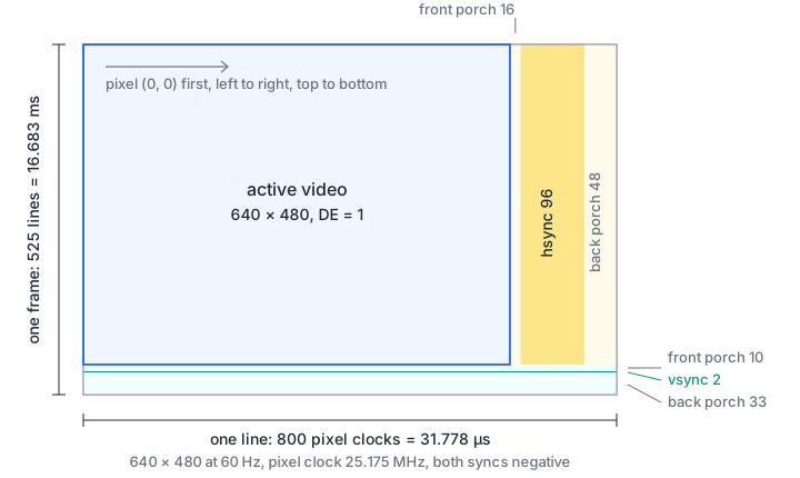
A video signal sends the picture one pixel at a time, left to right along a line and line by line from top to bottom. One pixel moves per cycle of the pixel clock. Each line has more clock cycles than visible pixels, and each frame has more lines than visible lines. The extra time is blanking. Digital links keep it and send synchronisation characters in it.
A line consists of four parts, in this order:
- Active video: the visible pixels.
- Front porch: blank pixels before the sync pulse.
- Horizontal sync (hsync): a pulse that marks the start of a new line.
- Back porch: blank pixels after the sync pulse, before the next line’s active video.
A frame has the same four parts, counted in whole lines: active lines, vertical front porch, vertical sync (vsync) and vertical back porch.
Each sync has a polarity. A negative sync idles high and pulses low; a positive sync idles low and pulses high. The polarities are part of each mode’s definition in the standard.
Digital interfaces add DE (data enable), high during active video and low during blanking. A DVI transmitter uses DE to decide whether to send pixel data or control characters.
Timing from the standard
Monitor timings for PC resolutions are collected in the VESA Display Monitor Timing (DMT) standard. Its 640 × 480 at 60 Hz entry (DMT version 1.0 rev. 13, page 21) is listed “for reference only”, as an industry-standard timing rather than a VESA standard. It gives:
- pixel clock 25.175 MHz ± 0.5 %, line rate 31.469 kHz, frame rate 59.940 Hz
- horizontal: 640 addressable pixels, 8-pixel right border, 8-pixel front porch, 96-pixel sync, 40-pixel back porch, 8-pixel left border, 800 in total
- vertical: 480 addressable lines, 8-line bottom border, 2-line front porch, 2-line sync, 25-line back porch, 8-line top border, 525 in total
- both syncs negative
The DMT counts the borders as part of the “active” video but not of the addressable picture (section 3, page 14). A digital source that raises DE only for the 640 × 480 addressable pixels sends them as blanking. Folding each border into its neighbouring porch gives the parameters used in this lesson’s generator: front porch 8 + 8 = 16, back porch 40 + 8 = 48, vertical front porch 8 + 2 = 10 and vertical back porch 25 + 8 = 33. The sync positions do not change: the horizontal sync still starts at pixel 656, as the DMT’s “Hor Sync Start” states.
The DMT also lists 1280 × 720 at 60 Hz (page 39), noted there as the CEA-861 720p timing (code 4). It has no borders:
| Mode | Pixel clock | H active / FP / sync / BP / total | V active / FP / sync / BP / total | Sync polarity | Frame rate |
|---|---|---|---|---|---|
| 640 × 480 @ 60 | 25.175 MHz | 640 / 16 / 96 / 48 / 800 | 480 / 10 / 2 / 33 / 525 | H−, V− | 59.940 Hz |
| 1280 × 720 @ 60 | 74.25 MHz | 1280 / 110 / 40 / 220 / 1650 | 720 / 5 / 5 / 20 / 750 | H+, V+ | 60.000 Hz |
Check the arithmetic: 25 175 000 / (800 × 525) = 59.940 Hz and 74 250 000 / (1650 × 750) = 60.000 Hz.
Generating the pixel clock
The pixel clock comes from a PLL (or an MMCM in AMD devices). A simple model of an FPGA PLL: the input is divided by D, multiplied by M in the voltage-controlled oscillator (VCO), and divided by O at the output:
Each device limits the VCO frequency and the divider ranges, and some restrict the dividers further (the iCE40 output divider, for example, is a power of two). Let the vendor’s clocking IP, or icepll from Project IceStorm for iCE40, choose the values, and check the output frequency it reports (icepll prints it as “achieved”).
Exact values are often impossible, so check the error. Some examples:
- 25.000 MHz is a common shortcut. It is 0.70 % below 25.175 MHz, outside the ± 0.5 % that the DMT gives. Some monitors may accept it, but the standard does not promise it.
- From 100 MHz, M = 36, D = 11, O = 13 gives 25.1748 MHz (VCO 327.3 MHz), an error of 0.0007 %.
- From 12 MHz, M = 99, D = 2, O = 8 gives exactly 74.25 MHz (VCO 594 MHz).
Whether a particular set of values is legal depends on your device’s clocking guide.
The pixel clock is usually a separate clock domain from the rest of the design. Anything that crosses into it, a mode register written by a processor or pixels from a frame buffer, needs the techniques from clock domain crossing.
The timing generator
video_timing.sv counts pixels in h_cnt and lines in v_cnt. All timing values are parameters, with 640 × 480 as the default:
assign h_act     = (h_cnt < XW'(H_ACTIVE));
assign v_act     = (v_cnt < YW'(V_ACTIVE));
assign h_sync_on = (h_cnt >= XW'(H_ACTIVE + H_FP)) && (h_cnt < XW'(H_ACTIVE + H_FP + H_SYNC));
assign v_sync_on = (v_cnt >= YW'(V_ACTIVE + V_FP)) && (v_cnt < YW'(V_ACTIVE + V_FP + V_SYNC));

always_ff @(posedge clk) begin
    ...
    hsync <= h_sync_on ? H_POL : ~H_POL;
    vsync <= v_sync_on ? V_POL : ~V_POL;
    de    <= h_act && v_act;
    x     <= h_cnt;
    y     <= v_cnt;
end
Counting starts at the first active pixel, so x and y equal the counters whenever DE is high. All outputs are registered, so they change together, one clock after the counters. The parameters H_POL and V_POL give the level of the sync pulse: 1 for positive, 0 for negative. In this generator, vsync changes at the start of a line.
The counter widths come from $clog2 of the totals: 10 bits for 800 and 525, 11 bits for 1650. A frame_start pulse marks the first pixel of each frame for downstream logic.
video_timing.sv
A test-pattern generator
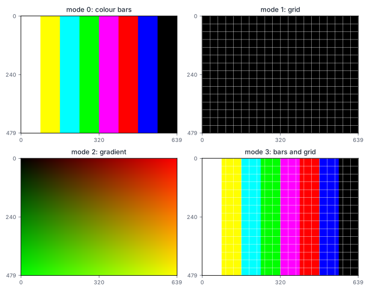
A known pattern is the quickest way to check a new video output. test_pattern.sv takes x, y and de and produces 8-bit red, green and blue one clock later:
| Mode | Pattern | What it shows |
|---|---|---|
| 0 | Eight colour bars | Colour channels swapped or missing |
| 1 | White grid every 32 pixels, with a one-pixel border | Cropped edges, scaling by the monitor |
| 2 | Gradient: red rises with x, green with y | Missing or stuck data bits |
| 3 | Bars with the grid on top | Both at once |
The bars run white, yellow, cyan, green, magenta, red, blue and black. With the BT.601 luma weights (0.299 R + 0.587 G + 0.114 B) that is falling brightness from left to right. The colour is the inverted bar index, with bit 2 driving green, bit 1 red and bit 0 blue:
always_comb begin
    bar = 3'd0;
    for (int k = 1; k < 8; k++)
        if (x >= XW'(k * BAR_W)) bar = 3'(k);
end
assign bars = {{8{~bar[1]}}, {8{~bar[2]}}, {8{~bar[0]}}};
Comparisons replace a divider by 80. Outside DE the output is black, because a transmitter ignores pixel data during blanking and a defined value makes waveforms easier to read.
video_top_tfp410.sv connects the two blocks. The pattern adds one clock, so the top level delays hsync, vsync and DE by one clock to stay aligned with the colour. It then registers every output, so all pins change on the same edge.
test_pattern.sv
Download video_top_tfp410.sv
Verifying the timing
tb_video_timing.sv runs two generators side by side, 640 × 480 at 25.175 MHz and 1280 × 720 at 74.25 MHz, for two frames each. A monitor module measures everything from the outputs alone: cycles per frame, hsync pulses per frame, DE pixels per line, active lines, front and back porch, hsync and vsync widths, lines before vsync, and the idle sync levels at the first pixel.
iverilog -g2012 -o sim tb_video_timing.sv video_timing.sv
vvp sim
1280x720@60: frame 1: 1280 x 720 active, 1650 x 750 total, frame period 16.667 ms
640x480@60: frame 1: 640 x 480 active, 800 x 525 total, frame period 16.683 ms
1280x720@60: frame 2: 1280 x 720 active, 1650 x 750 total, frame period 16.667 ms
640x480@60: frame 2: 640 x 480 active, 800 x 525 total, frame period 16.683 ms
PASSThe run takes about 7 s in Icarus Verilog. The measured frame periods match the DMT’s 16.683 ms and 16.667 ms. If the DUT’s porches are changed to 17 and 47 while the monitor still expects 16 and 48, every active line reports a front-porch and a back-porch error.
The pattern is checked by cocotb. cocotb_video_top.py runs video_top_tfp410 with a small raster (64 × 24 visible, so it finishes in a second), captures two frames for each mode from the output pins, checks the sync widths and the front porch, rebuilds the picture from the DE-qualified pixels and compares it with pattern_model.py. Swapping two colour bits, or forgetting the one-clock delay on DE, makes it fail.
tb_video_timing.sv
Download cocotb_video_top.py
Download pattern_model.py
Download test_cocotb_video.py
Two ways to reach the HDMI connector
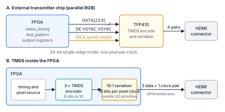
Option A: a TFP410 transmitter
The TI TFP410 is a DVI 1.0 transmitter. Its data sheet (SLDS145D) lists “HDMI video-only” among its applications, so it puts a picture on an HDMI connector but no audio. The course’s student kit drives its HDMI output through one.
The facts you need from the data sheet:
- Input bus. In 24-bit single-edge mode, DATA[23:16] is red, DATA[15:8] green and DATA[7:0] blue. DE, HSYNC and VSYNC are latched with the data.
- Clock. IDCK is the pixel clock, from 25 MHz to 165 MHz. The data sheet’s input options include a 12-bit dual-edge mode, which needs fewer pins.
- Configuration. With ISEL low, pins set the mode: BSEL high selects 24-bit single-edge input, EDGE selects whether data is latched on the rising (1) or falling (0) edge of IDCK, and PD high selects normal operation. With ISEL high, the same settings come from I2C registers, and the device starts powered down until software writes the PD bit.
- Timing. In single-edge mode the inputs need 1.2 ns setup and 1.3 ns hold time at IDCK.
- Outputs. Channel 0 carries blue, and HSYNC and VSYNC during blanking; channel 1 carries green and channel 2 red. A fourth pair carries the clock.
A simple, safe arrangement is to launch the data on the rising edge of the pixel clock and let the TFP410 latch on the falling edge (EDGE = 0). The data then has half a period of setup and of hold, nominally 19.9 ns at 25.175 MHz and 6.7 ns at 74.25 MHz, before output delays and board skew. Forward the clock with the device’s DDR output register (one input tied high, the other low) rather than routing the clock net straight to a pin. Your board decides how the configuration pins are strapped, so read its manual before you choose EDGE.
Option B: TMDS inside the FPGA
Without a transmitter chip, the FPGA must produce the TMDS signals itself. The DVI 1.0 specification defines them:
- Three data channels and a clock channel. Channel 0 carries blue, with HSYNC and VSYNC as its control inputs C0 and C1; channel 1 carries green and channel 2 red. The transmitter must hold their control inputs CTL1 to CTL3 low, and should hold CTL0 low.
- Each data channel sends one 10-bit character per pixel clock. The specification defines the bit time as one tenth of the pixel time, so at 25.175 MHz each lane runs at 251.75 Mbit/s and at 74.25 MHz at 742.5 Mbit/s.
- During blanking (DE low) the encoder sends one of four control characters, selected by C1 and C0. A receiver must establish synchronisation during any blanking period longer than 128 characters.
- During active video the encoder works in two stages.
Stage 1, fewer transitions. The first output bit equals the first data bit. Every next bit is the previous output bit XOR the next data bit, or XNOR if the data byte has more than four ones (or exactly four with bit 0 clear). A ninth bit records which was used:
assign use_xnor = (ones(d) > 4'd4) || (ones(d) == 4'd4 && d[0] == 1'b0);
assign q_lo     = use_xnor ? xn_chain : x_chain;     // q_m[7:0]
assign q_m8     = ~use_xnor;                         // q_m[8]
Stage 2, DC balance. A counter cnt tracks the running disparity, the excess of ones over zeros already sent. If the new word would push the disparity further from zero, the encoder inverts the eight data bits and sets the tenth bit:
end else if ((cnt > 0 && diff > 0) || (cnt < 0 && diff < 0)) begin
    q_next   = {1'b1, q_m8, ~q_lo};                // invert to pull cnt back
    cnt_next = cnt + (q_m8 ? 6'sd2 : 6'sd0) - diff;
diff is the number of ones minus zeros in q_m[7:0]. The receiver undoes both steps with the two flag bits. The serialiser sends q_out[0] first.
tmds_model.py transcribes figure 3-5 of the specification line by line, with bit lists indexed like the specification. Its tests check three properties: active data uses exactly 460 different characters, the number the specification states, none equal to a control character; every character decodes back to its byte; and in a 200 000-character random run the running disparity stays within ±8. The first stage leaves at most 3 transitions in the eight data bits, against up to 7 in raw data. cocotb_tmds_encoder.py drives 400 bursts of active and blanking characters, about half of them a repeated constant value that stresses the DC balance, and compares every output character with the model.
The serialiser is device-specific. It shifts out 10 bits per pixel clock, using the device’s serialiser primitive or IP, and drives differential output pins on an I/O standard the device and board support for TMDS. Check both in your device’s I/O guide and your board’s schematic. That is why this lesson verifies the encoder but does not ship a serialiser.
Downloadtmds_encoder.sv
Download tmds_model.py
Download test_tmds_model.py
Download cocotb_tmds_encoder.py
Run all Python and cocotb tests in the lesson folder with python -m pytest -q (8 tests, about 4 s).
Add 800 × 600 at 60 Hz
The DMT entry for 800 × 600 at 60 Hz (page 26) lists: pixel clock 40.000 MHz, 800 addressable pixels, front porch 40, sync 128, back porch 88, 1056 in total; 600 addressable lines, front porch 1, sync 4, back porch 23, 628 in total; no borders; both syncs positive.
- Write the parameter list for
video_timing. - What are the line rate, frame rate and TMDS bit rate per lane?
- How wide are the
xandyoutputs?
Show solution
The parameters:
video_timing #(
    .H_ACTIVE(800), .H_FP(40), .H_SYNC(128), .H_BP(88),
    .V_ACTIVE(600), .V_FP(1),  .V_SYNC(4),   .V_BP(23),
    .H_POL(1'b1),   .V_POL(1'b1)
) u_svga (...);
Line rate 40 000 000 / 1056 = 37.879 kHz; frame rate 37 879 / 628 = 60.317 Hz, both as the DMT lists. Each TMDS lane runs at 10 × 40 MHz = 400 Mbit/s. x is $clog2(1056) = 11 bits wide and y is $clog2(628) = 10 bits wide.
Running the timing testbench with these values (both monitor and generator, clock period 25 ns) prints 800 x 600 active, 1056 x 628 total, frame period 16.579 ms and PASS. A 40 MHz clock is easy to make exactly: from 100 MHz, M = 8, D = 1, O = 20 (VCO 800 MHz).
Check a TMDS character by hand
Encode the byte 0x00 with the running disparity at zero and DE high.
Show solution
The byte has no ones, so stage 1 uses XOR. q_m[0] = 0 and every XOR with 0 keeps 0, so q_m[7:0] = 0000 0000 and q_m[8] = 1.
Stage 2: the disparity is zero, so the first branch applies. q_m[8] = 1, so the data bits are sent unchanged, q_out[8] = 1 and q_out[9] = 0. The character, written q_out[9:0], is 01 0000 0000 = 0x100. The disparity becomes 0 + (0 - 8) = -8.
Encode 0x00 again: the disparity is now negative and the word has more zeros than ones, so the inversion branch applies. q_out[7:0] = 1111 1111, q_out[8] = 1, q_out[9] = 1, giving 0x3FF, and the disparity becomes -8 + 2 + 8 = +2. The model in tmds_model.py gives the same two characters.
Summary
- A raster line is active video, front porch, sync and back porch; a frame is the same in whole lines. DE marks the visible pixels, and each sync has a defined polarity.
- Take timing values from the VESA DMT: 640 × 480 at 60 Hz is 800 × 525 clocks at 25.175 MHz with negative syncs, 1280 × 720 at 60 Hz is 1650 × 750 at 74.25 MHz with positive syncs. Fold DMT borders into the porches.
- Make the pixel clock with a PLL and check the error against the DMT’s ± 0.5 %; 25.000 MHz is 0.70 % low.
- A parameterised counter pair with registered outputs generates the timing, and a self-checking testbench can measure every interval from the outputs alone.
- A TFP410 takes 24-bit RGB with DE, syncs and the pixel clock, and does the TMDS work. Without it, the FPGA needs three DVI TMDS encoders plus 10:1 serialisers on suitable differential pins.
Check your understanding
Pick an answer for each question, then check. Answers stay hidden until you submit.
Further reading
- Standard
- Standard
- Documentation
Found a mistake or something unclear?Report a correction.
Follow this course
Get an email when new lessons and projects are added to this course.