Week 6 · Timing, clocks and implementation · Lesson 11 of 24
Static timing analysis and timing closure for FPGAs
How static timing analysis checks setup and hold, how to write SDC and XDC timing constraints, read WNS, TNS and WHS in a timing report, and fix failing paths.
What you will learn
- Write the setup and hold inequalities for a register-to-register path, including clock skew and uncertainty
- Calculate setup slack and Fmax for a path from its delay components
- Constrain clocks, I/O delays and timing exceptions in SDC and XDC
- Read WNS, TNS and WHS in a timing summary and find the failing path
- Choose a fix for a failing path: pipelining, retiming, fewer logic levels, lower fanout or floorplanning
Before you start
- Sequential logic (lesson 7)
- FPGA architecture (lesson 2)
- The FPGA design flow (lesson 3)
After this lesson you can calculate whether a register-to-register path meets timing, write the constraints that tell the tools what “meets timing” means for your design, and read the timing report that comes back. You will also know the usual fixes for a failing path and in which order to try them.
What static timing analysis does
A simulator checks function, not delay. Static timing analysis (STA) uses the delay of every cell and routed net after place and route, adds them up along each path, and compares the total with the clock requirement. No test vectors are involved, so every path is checked, not only the ones a testbench exercises. The result is only as good as your constraints: a path with no clock on it is not checked at all.
Delays are characterised at slow and fast process, voltage and temperature corners. Setup is usually limited by the slow corner and hold by the fast corner, and the tools check both.
Anatomy of a register-to-register path
Most paths in a synchronous design start at one flip-flop and end at another (see sequential logic). Registers break the design into small combinational pieces with a clock edge at each end. The figure shows the parts of one such path.
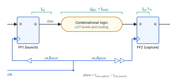
The delays are:
- Clock-to-Q, : time from the launch clock edge at FF1 to a valid output.
- Logic delay, : the LUTs, carry chains and other cells between the registers. Each LUT the signal passes through is one logic level.
- Routing delay, : the programmable interconnect between those cells. On FPGAs it is often a large share of the total, which is why placement matters.
- Setup time, : how long before the capture edge the data at FF2 must be stable.
- Hold time, : how long after the capture edge the data at FF2 must stay stable.
- Clock arrival times, and : delay from the clock source to each flip-flop’s clock pin.
The clock skew is the difference in clock arrival:
The clock uncertainty is a margin for jitter and similar cycle-to-cycle variation. Vivado calculates it from the clock jitter (system jitter, input jitter and the jitter added by an MMCM or PLL); Quartus Prime Lite and Standard add it when the SDC file calls derive_clock_uncertainty. set_clock_uncertainty adds more.
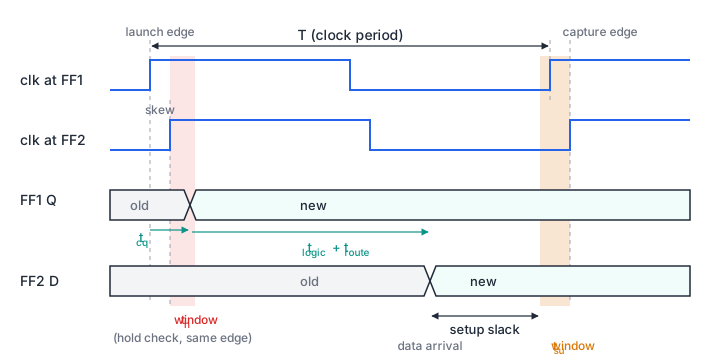
The setup check
Data launched by one clock edge must arrive at FF2 at least before the next capture edge, one clock period later. Measured from the same clock source:
Subtract from both sides and the setup condition becomes:
Slack is the margin: required time minus arrival time. Positive slack means the path passes. Negative slack means it fails by that amount.
Positive skew (capture clock later) gives the data more time and helps setup.
The hold check
The hold check protects FF2 from the same clock edge that launched the data. When FF1 launches new data, FF2 is capturing the old data on that same edge. The new data must not reach FF2 until after the capture clock arrives there:
The clock period does not appear, so changing the clock frequency never fixes a hold violation. Positive skew hurts hold. The router fixes most hold problems by adding delay to fast paths, provided the skew is small. Hold failures that remain usually point to a clock problem, such as a clock routed through general logic instead of a dedicated clock network.
Worked example at 100 MHz
The numbers below are example values chosen to show the arithmetic. They are not taken from a specific device.
Assume a 100 MHz clock, so ns. The timing analyser reports these delays for the slowest path:
| Quantity | Value |
|---|---|
| Launch clock arrival, | 2.10 ns |
| Capture clock arrival, | 1.90 ns |
| Clock-to-Q, | 0.45 ns |
| Logic delay, (4 LUT levels) | 3.10 ns |
| Routing delay, | 4.25 ns |
| Setup time, | 0.10 ns |
| Clock uncertainty, | 0.15 ns |
The skew is ns. The capture clock arrives early, which costs setup margin.
Data arrival time: ns.
Data required time: ns.
Setup slack: ns. The path passes.
Fmax
The path would still pass with a period 1.75 ns shorter. For a single-clock design whose worst path is a normal one-cycle register-to-register path:
This is an estimate, because a run at a tighter clock gives a different placement. Quartus reports a per-clock “Fmax Summary”; in Vivado you calculate it from WNS as above.
Hold on the same pair of registers
The hold check uses the fastest delays, from the fast corner. Assume (again example values) a shortest path of ns and ns. At the fast corner the clock arrives at 1.40 ns at FF1 and 1.55 ns at FF2, so the skew is +0.15 ns. With ns and a hold uncertainty of 0.05 ns:
Hold slack ns.
Input and output delays
For a path to or from a pin, the other register sits in an external chip. You describe the outside part of the path, relative to a clock, with two commands:
- Input delay: external clock-to-output time plus board trace delay. The
-maxvalue drives the setup check and-minthe hold check. - Output delay: external setup time plus trace delay for
-max; trace delay minus external hold time for-min, which is often negative.
Example values: an ADC launches data on the same 100 MHz clock with a clock-to-output time of 1.0 ns to 3.0 ns and a trace delay of 0.3 ns to 0.5 ns. A DAC needs 2.0 ns of setup and 0.5 ns of hold, with 0.2 ns to 0.4 ns of trace delay.
# Example values; take the real numbers from the data sheets and the board layout.
create_clock -name sys_clk -period 10.000 [get_ports clk]

# ADC -> FPGA: max = 3.0 + 0.5, min = 1.0 + 0.3
set_input_delay  -clock sys_clk -max  3.5 [get_ports {adc_data[*]}]
set_input_delay  -clock sys_clk -min  1.3 [get_ports {adc_data[*]}]

# FPGA -> DAC: max = 2.0 + 0.4, min = 0.2 - 0.5
set_output_delay -clock sys_clk -max  2.4 [get_ports {dac_data[*]}]
set_output_delay -clock sys_clk -min -0.3 [get_ports {dac_data[*]}]
This model assumes the clock reaches both chips at the same time; on a real board, include the clock trace difference. The commands are the same in Vivado and Quartus. Registers placed in the I/O cells give the same pin-to-register delay on every build.
Writing constraints
Both Vivado and Quartus use the Synopsys Design Constraints (SDC) command set. Vivado stores constraints in .xdc files, which hold SDC timing commands plus Vivado-specific physical properties such as pin locations. Quartus reads timing constraints from .sdc files and keeps pin and device settings in the .qsf project file.
The main differences you will meet:
| Topic | Vivado (XDC) | Quartus (SDC) |
|---|---|---|
| Hierarchy separator in names | /, e.g. u_core/cnt_reg[3] | |, e.g. u_core|cnt[3] |
| Object queries | get_cells, get_pins, get_nets, get_ports, get_clocks | get_registers, get_keepers, get_pins, get_nets, get_ports, get_clocks |
| PLL/MMCM output clocks | Created automatically from the input clock | Lite and Standard: derive_pll_clocks in the SDC file |
| Clock uncertainty | Calculated automatically | Lite and Standard: derive_clock_uncertainty in the SDC file |
| Path delay without clock skew | set_max_delay -datapath_only | No -datapath_only option |
The open-source nextpnr flow takes a target frequency per clock (for example with its --freq option) and reports the achieved Fmax, but it does not support the full SDC command set.
Clocks
Every clock that enters the FPGA needs a create_clock on its pin:
create_clock -name sys_clk -period 10.000 -waveform {0.000 5.000} [get_ports clk]-waveform gives the rising and falling edge times; {0 5} is the default 50 % duty cycle for a 10 ns period.
Clocks made inside the FPGA need create_generated_clock, so the analyser knows their relation to the source clock. Vivado creates MMCM and PLL output clocks automatically, and in Quartus Prime Lite and Standard derive_pll_clocks does the same. A clock divided in fabric logic must be declared by hand:
# Vivado: a divide-by-2 clock from register clk_div_reg
create_generated_clock -name clk_div2 -source [get_pins clk_div_reg/C] \
    -divide_by 2 [get_pins clk_div_reg/Q]

# Quartus: the same register, Quartus naming
create_generated_clock -name clk_div2 -source [get_pins {clk_div|clk}] \
    -divide_by 2 [get_pins {clk_div|q}]
A clock from a fabric register leaves the dedicated clock network and adds skew. Use a PLL or MMCM output, or a clock enable on the fast clock, instead. Clock domain crossing covers what happens at the boundary between clocks.
False paths
set_false_path removes paths from analysis. Use it only where timing does not matter, such as a push button that enters a synchroniser:
set_false_path -from [get_ports btn_raw]Multicycle paths
Sometimes data only needs to arrive every second cycle, because the destination register has a clock enable that is high every other cycle. A multicycle constraint relaxes the setup check to N cycles. It must be paired with a hold constraint of N - 1, otherwise the hold check moves out with the setup edge:
# Vivado: setup over 2 cycles, hold back to the launch edge
set_multicycle_path 2 -setup -from [get_cells {acc_reg[*]}] -to [get_cells {result_reg[*]}]
set_multicycle_path 1 -hold  -end -from [get_cells {acc_reg[*]}] -to [get_cells {result_reg[*]}]

# Quartus: same constraint, Quartus naming
set_multicycle_path -setup -end -from [get_registers {acc[*]}] -to [get_registers {result[*]}] 2
set_multicycle_path -hold  -end -from [get_registers {acc[*]}] -to [get_registers {result[*]}] 1
The constraint is only correct if the RTL guarantees it. If the enable logic changes, the constraint becomes a lie the tools cannot detect.
Clock groups
set_clock_groups -asynchronous tells the analyser that two sets of clocks have no phase relation, so it does not time paths between them:
set_clock_groups -asynchronous -group [get_clocks sys_clk] -group [get_clocks eth_rx_clk]Use it only when every crossing between the groups goes through a proper synchroniser. The clock domain crossing lesson shows the synchronisers and the CDC-specific constraints that go with them.
Checking the constraints
After every constraint change, run check_timing in Vivado or the “Unconstrained Paths” report in Quartus. Fix unclocked registers and I/O without delays before you read any slack numbers.
Reading a timing report
Start with the summary. Vivado’s report_timing_summary gives these numbers:
- WNS (worst negative slack): the smallest setup slack of all paths. Zero or positive means every setup check passes.
- TNS (total negative slack): the sum of the negative setup slacks over all failing endpoints. It shows whether you have one bad path or thousands.
- WHS (worst hold slack) and THS (total hold slack): the same for hold.
Quartus shows setup and hold summaries per clock and per corner, with the worst slack and the “End Point TNS” for each clock. In either tool, timing is met only when WNS and WHS are both zero or positive at every corner and every clock.
Then open the worst path. The detailed report lists every cell and net with its delay. For the worked example, the key lines look like this (simplified, not literal tool output):
Slack (MET):        1.750 ns
Source:             u_core/acc_reg[7]/C   (rising edge sys_clk)
Destination:        u_core/sum_reg[15]/D  (rising edge sys_clk)
Requirement:        10.000 ns
Data path delay:    7.800 ns  (logic 3.550 ns 45.5%, route 4.250 ns 54.5%)
Logic levels:       4
Clock path skew:    -0.200 ns
Clock uncertainty:  0.150 ns
Here clock-to-Q counts as logic (0.45 + 3.10 = 3.55 ns). The logic levels, the route percentage and the skew tell you which fix to try.
Fixing failing paths
Work through these in order. The first ones change the RTL and give the largest gains; the last ones only work around a placement problem.
1. Pipeline the path
Add registers to split a long path into shorter ones. You pay with latency, so the surrounding logic must accept the extra cycles. The download below sums eight 16-bit numbers two ways. sum8_chain.sv registers the inputs and output and puts seven adders in series between them. sum8_pipe.sv uses a balanced adder tree with a register after each level, so each register-to-register path holds a single adder:
always_ff @(posedge clk) begin
    x_r <= x;
    for (int i = 0; i < 4; i++) begin
        s1[i] <= (W+1)'(x_r[2*i]) + (W+1)'(x_r[2*i+1]);
    end
    for (int i = 0; i < 2; i++) begin
        s2[i] <= (W+2)'(s1[2*i]) + (W+2)'(s1[2*i+1]);
    end
    y <= (W+3)'(s2[0]) + (W+3)'(s2[1]);
end
Latency grows from 2 to 4 cycles. The valid signal travels through a shift register of the same length, so downstream logic knows when y is ready. The testbench feeds both versions the same random inputs and checks both against a reference sum.
sum8_chain.sv
Download sum8_pipe.sv
Download tb_sum8.sv
iverilog -g2012 -o sim tb_sum8.sv sum8_chain.sv sum8_pipe.sv && vvp sim
# PASS: 798 sums checked on each design
2. Let the tool retime
Retiming moves existing registers across combinational logic to balance the delays on either side, without changing the outputs. A common pattern is to add a few registers at the end of a path and let the tool push them back into the logic. Vivado supports retiming during synthesis (synth_design -retiming) and in physical optimisation. Quartus has register retiming options, and Quartus Prime Pro adds Hyper-Retiming for devices with the Hyperflex architecture (Stratix 10 and Agilex 7). Asynchronous resets and registers that must be preserved, such as synchronisers, limit what the tool can move.
3. Reduce logic levels
Common causes of deep logic:
- Long
if/else ifpriority chains where the conditions are mutually exclusive. Acasestatement or a parallel AND-OR structure is shallower. - Wide comparisons against a terminal count. Register an “almost done” flag one cycle early instead.
- Arithmetic followed by more arithmetic in the same cycle, as in the chain example.
Vivado’s report_design_analysis shows the logic-level distribution of the worst paths, which tells you whether the problem is one path or a pattern.
4. Reduce fanout
A signal with hundreds of loads (a pipeline enable, a reset, a state bit) has a long, spread-out net whose routing delay dominates. Duplicate the source register so each copy drives a local group of loads. The MAX_FANOUT attribute in Vivado and the maximum fanout assignment in Quartus ask the tool to do this, and Vivado’s physical optimisation also replicates high-fanout drivers. For reset nets, reset only the registers that need a known start value (control state, valid flags).
5. Floorplan, as a last resort
If the logic is shallow but the route percentage is high, the cells are placed far apart, for example because a block connects to I/O on opposite sides of the die. Floorplanning (Pblocks in Vivado, Logic Lock regions in Quartus) confines logic to a region. It also takes freedom away from the placer, and a bad floorplan makes timing worse. Try it only after the RTL and constraint fixes, and keep the regions generous. If the system allows it, a lower clock frequency is also a legitimate fix.
Calculate slack and Fmax
A path has these example values: ns, ns, ns, ns, launch clock arrival 1.50 ns, capture clock arrival 1.62 ns, clock uncertainty 0.12 ns. The clock is 150 MHz.
- Calculate the setup slack.
- Estimate Fmax for this path.
- The shortest path into the same register has ns at the fast corner, with the same skew, ns and a hold uncertainty of 0.03 ns. Does it meet hold?
Show solution
- ns. Skew ns. Data path ns. Setup slack ns. The path passes.
- MHz.
- Hold slack ns. It fails by 20 ps. The positive skew that helped setup hurts hold here. The router normally fixes a violation this small by adding delay to the short path; if it cannot, check why the skew is positive (for example, a clock that leaves the dedicated clock network).
Constrain a multicycle path
A 32-bit divider in your design takes its inputs from registers div_a and div_b and writes div_q. A control FSM loads the inputs and enables div_q only every fourth cycle of the 200 MHz clock clk_core. Write the Vivado constraints that relax the path, and state what you must check in the RTL before you trust them.
Show solution
set_multicycle_path 4 -setup -from [get_cells {div_a_reg[*] div_b_reg[*]}] -to [get_cells {div_q_reg[*]}]
set_multicycle_path 3 -hold  -end -from [get_cells {div_a_reg[*] div_b_reg[*]}] -to [get_cells {div_q_reg[*]}]
The setup multiplier is 4 and the hold multiplier is 4 - 1 = 3, which brings the hold check back to the launch edge. Before trusting the constraint, check that div_a and div_b never change during the four cycles before div_q is enabled, and that the enable of div_q is high only on the fourth cycle. An assertion in simulation is cheap insurance. If the FSM is changed to load faster, the constraint must change with it.
Summary
- Static timing analysis adds up cell and routing delays on every path and compares them with the clock constraints. Paths without constraints are not checked.
- Setup requires . Hold requires the data path to be longer than plus uncertainty, and does not depend on the clock period.
- Slack is required time minus arrival time. WNS and TNS summarise setup; WHS and THS summarise hold. Timing is met when WNS and WHS are zero or positive at every corner.
- Constrain every clock with
create_clockorcreate_generated_clock, every synchronous I/O with input and output delays, and add exceptions (false paths, multicycle paths, clock groups) only where the RTL guarantees them. - Fix failing paths in this order: pipeline, retime, reduce logic levels, reduce fanout, and floorplan only as a last resort.
Check your understanding
Pick an answer for each question, then check. Answers stay hidden until you submit.
Further reading
- Documentation
- Documentation
- Documentation
Found a mistake or something unclear?Report a correction.
Follow this course
Get an email when new lessons and projects are added to this course.